
Applications
Thanks to its innovative technology and unique features, major companies in the electronics and semiconductor industries have chosen the TDM system for both quality control and R&D purposes. Our customers appreciate the technical advantages of the TDM system, including its high-resolution sensor, system versatility, and user-friendly interface.
The TDM system is a versatile instrument suited for a wide array of applications, including:
Product & Process Development
Failure Analysis
Reliability Testing
Quality Control
Whether you are enhancing your production processes or conducting in-depth research, the TDM system provides the precision and flexibility needed to achieve your goals.
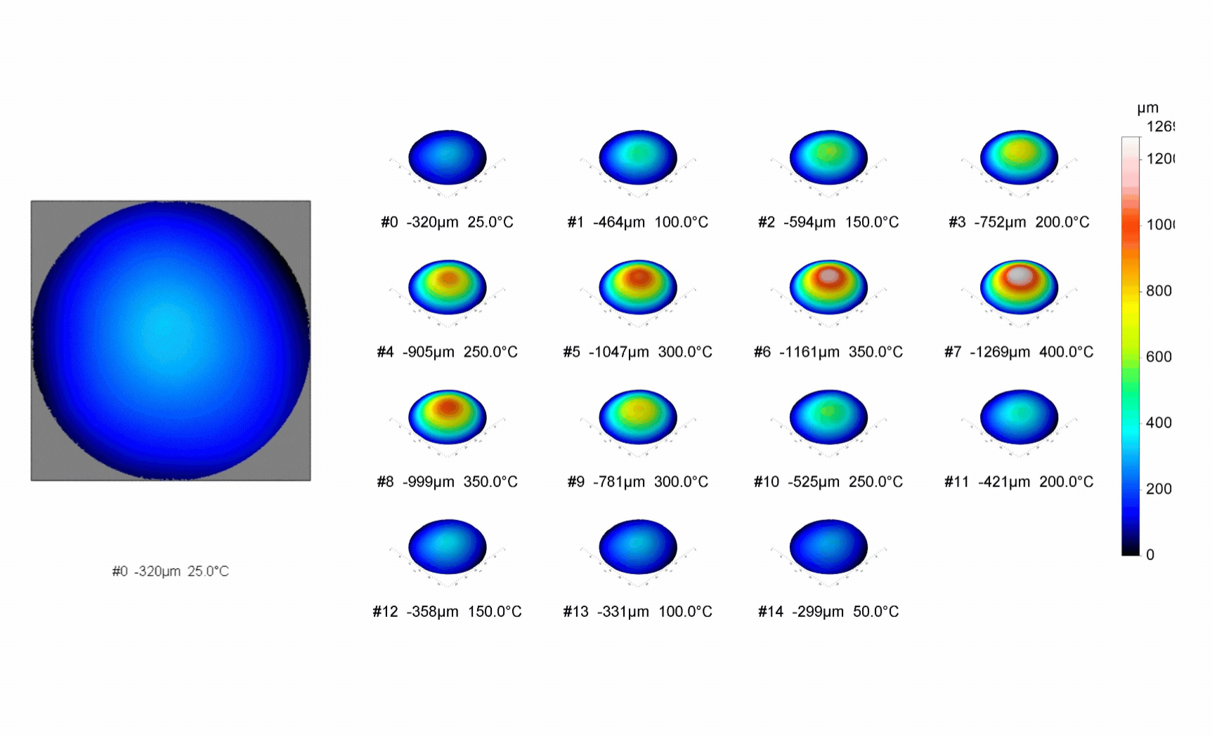
Wafers
Temperature measurement range: 25℃ to 400℃ to 25℃
Field of View 300
Wafer Thermal Warpage Measurement
Ensure Material Integrity and Performance: prevent mechanical stress and potential defects in Si, SiC, and GaN wafers by monitoring and controlling thermal warpage.
Enhance Manufacturing Precision: achieve accurate pattern transfer in lithography processes and ensure high yield and quality in semiconductor manufacturing by minimizing warpage.
Improve Device Reliability and Lifespan: reduce the risk of early device failures and enhance the reliability and longevity of semiconductor devices through precise warpage monitoring.
Optimize Process and Reduce Costs: enable real-time process adjustments, enhance quality control, and reduce waste and rework costs by continuously monitoring wafer warpage.
Advance Research and Development: gain insights into the warpage behavior of different materials under thermal stress, aiding in the development of new materials and processes, and pushing the boundaries of semiconductor technology.

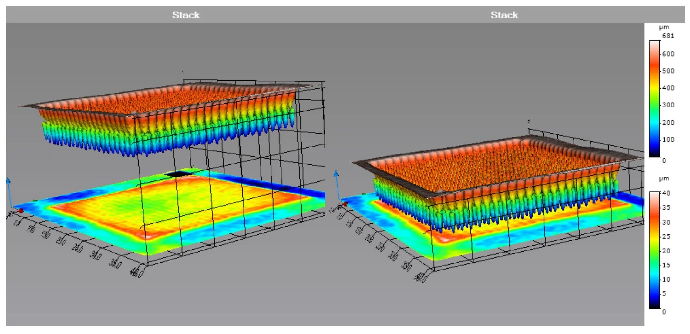
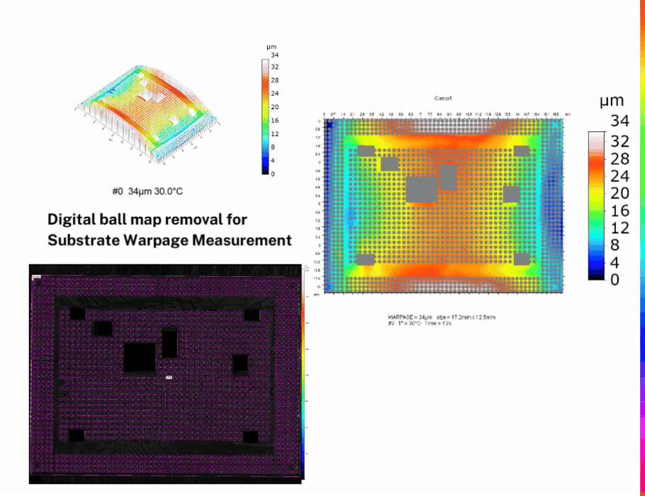
Ball Grid Arrays
Temperature measurement range: 25℃ to 260℃ to 25℃
Field of View: 30
Maximum warpage of: 52 µm detected
The Use of TDM Systems for BGAs
Ensure Reliable Solder Joints: monitoring thermal warpage helps maintain the integrity of solder joints, crucial for BGAs due to their lack of mechanical compliance compared to leaded components.
Mitigate Thermal and Mechanical Stress: accurate measurement of thermal warpage helps manufacturers address and reduce the risks of thermal and mechanical stress-induced fractures, enhancing the durability of BGA components.
Enhance Process Optimization: real-time thermal warpage data allows for fine-tuning manufacturing processes, ensuring that BGAs and PCBs match mechanical and thermal characteristics, reducing the occurrence of defects.
Improve Quality Control: continuous monitoring ensures high-quality production by detecting and addressing warpage issues early, thereby preventing faulty BGAs from reaching the end product.
Facilitate Research and Development: understanding the warpage behavior of BGAs under different conditions aids in developing more robust packaging solutions and improving overall BGA technology.
In Situ Measurement Capability: Insidix's TDM system allows for real-time, in situ thermal warpage measurement, providing immediate feedback during the manufacturing process, critical for maintaining the flatness and reliability of BGAs.
Address Thermal Expansion Issues: BGAs often suffer from thermal expansion mismatches between the PCB and the package. The TDM system helps in identifying and mitigating these mismatches, preventing thermal stress-induced failures.
Enhanced Reliability with Lead-Free Solder: the use of RoHS-compliant lead-free solder presents challenges like "head in pillow" and "pad cratering." TDM systems help in monitoring and controlling warpage to ensure reliable solder joints, even with less ductile lead-free solders.
Support for Advanced Packaging Solutions: techniques like underfilling and compliant layers are used to overcome mechanical stress in BGAs. TDM systems provide precise measurements necessary for optimizing these techniques, ensuring that they effectively enhance BGA reliability.
Critical for High-Performance Applications: In extreme operating conditions (high temperature, thermal shock, gravitational forces), the reliability of BGAs is paramount. TDM systems help ensure that BGAs maintain their integrity and performance under such conditions.
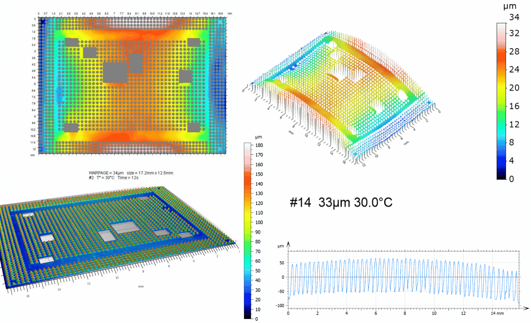
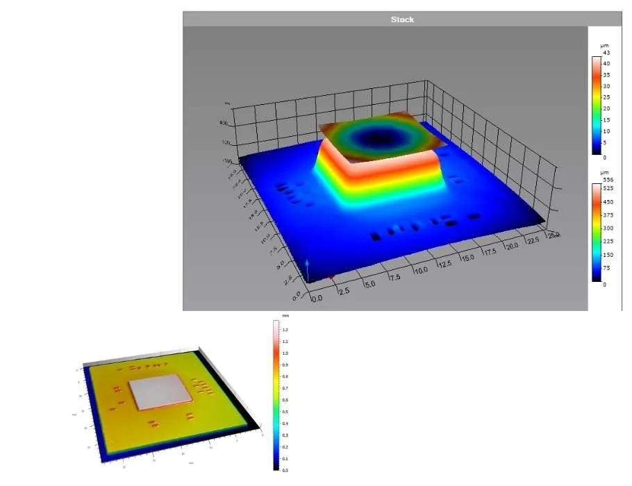
Stiffener on Flip Chip
Complaint warpage measurement with JEDEC JESD22-B112 + Preconditioning
From 30°C - 260°C Warpages = up to 405µm (3D image)
FOV70
Enhance Stiffener and Package Integrity with TDM
Prevent Stiffener Fracture: Accurate monitoring of thermal warpage helps identify and mitigate stress concentrations that can lead to stiffener fracture, ensuring the structural integrity of the package.
Maintain Package Flatness: By controlling stiffener warpage, TDM systems maintain overall package flatness, which is crucial for optimal solder joint formation and electrical performance.
Control: continuous monitoring ensures high-quality production by detecting and addressing warpage issues early, thereby preventing faulty devices from reaching the end product.
Facilitate Research and Development: understanding the warpage behavior of BGAs under different conditions aids in developing more robust packaging solutions and improving overall BGA technology.
Fine-tune Stiffener Design: Real-time warpage data enables iterative design improvements, leading to better-optimized stiffeners for thermal and mechanical performance.
Improve Assembly Yield: Precise warpage control contributes to higher assembly yields by reducing the incidence of misalignment, voids, and other defects related to stiffener deformation.
Reduce Stress on Solder Joints: Minimizing stiffener warpage helps to distribute stress evenly across solder joints, preventing premature failure and enhancing product lifespan.
Enhance Thermal Cycling Performance: TDM-enabled warpage control improves a package's ability to withstand repeated thermal cycles, critical for applications in harsh environments.
Enhance Thermal Cycling Performance: TDM-enabled warpage control improves a package's ability to withstand repeated thermal cycles, critical for applications in harsh environments.
Enable Thin and Flexible Packages: TDM systems provide the necessary data to optimize stiffener design for thin and flexible packages, where warpage control is paramount.
Facilitate Underfill Optimization: Accurate warpage measurement helps determine the optimal underfill material and curing process to minimize stress and enhance reliability.
Real-Time Feedback: Insidix's TDM system offers real-time warpage data, enabling immediate process adjustments to prevent defects and ensure product quality.
Identify Root Causes: By correlating warpage data with other process parameters, TDM helps pinpoint the root causes of warpage-related issues.

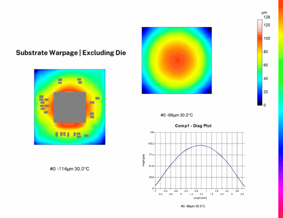
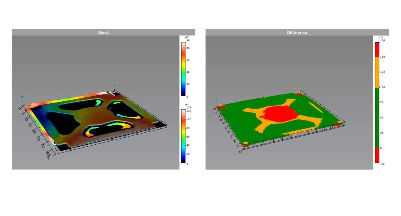
Underfill Flip Chip
Room Temp to 250°C
Die Warpages up to 128µm (2D image) Substrate Warpage up to 103µm
FOV20
Understanding the Role of TDM in Flip Chip Technology
TDM is an excellent tool for optimizing flip-chip component performance. By accurately measuring warpage, TDM can significantly contribute to:
Improved Electrical Performance
Predicting Solder Joint Reliability: TDM can help assess the stress on solder joints during thermal cycling. This information can be used to optimize solder joint design and material selection, ensuring reliable electrical connections.
Coplanarity Control: Accurate warpage measurement helps maintain optimal coplanarity between the chip and the substrate, minimizing signal distortion and crosstalk.
Higher Packaging Density
Underfill Optimization: TDM can evaluate the effectiveness of underfill materials in mitigating warpage. Engineers can optimize underfill thickness and material selection to achieve higher packaging density by understanding the underfill's CTE impact on warpage.
Component Placement Accuracy: Precise warpage data can improve component placement accuracy, enabling smaller package sizes and increase I/O counts.
Better Thermal Management
Thermal Stress Analysis: TDM can help identify areas of high thermal stress in the flip chip package. This information can be used to optimize heat sink design and placement for efficient heat dissipation.
Warpage-Induced Stress on Components: By quantifying warpage, TDM can help assess the impact of thermal expansion on component stress, preventing premature failure.
Specific TDM Applications for Flip Chip
Underfill Curing Optimization: TDM can monitor warpage changes during the underfill curing process to determine the optimal curing conditions.
Thermal Cycling Testing: TDM can evaluate the long-term reliability of flip chip components by measuring warpage before and after thermal cycling.
Failure Analysis: TDM can be used to analyze failed components to identify warpage-related issues and implement corrective actions.
Ball Grid Arrays
TDM is a critical tool for controlling warpage in microelectronics
Warpage, caused by thermal expansion mismatch, affects component coplanarity and solder joint reliability.
TDM precisely measures warpage, enabling optimization of materials, design, and manufacturing processes.
Key TDM features include phase shifting projection moiré, interferometry, comprehensive temperature range testing, and alignment with industry standards.
TDM addresses the increasing demand for accurate warpage measurement in advanced microelectronics packaging.
TDM Application to Ball Grid Arrays (BGAs)
Warpage in Flip-Chip Ball Grid Array (FCBGA) packages is a significant reliability concern.
Studies have shown that warpage varies across the package and is influenced by material properties and temperature.
Accurate material characterization is crucial for reliable warpage simulations.
Both thermal expansion and chemical shrinkage during post-mold curing (PMC) contribute to BGA warpage.
Coupled chemical-thermo-mechanical models are necessary for precise warpage prediction.
TDM is essential for addressing warpage challenges in BGAs and other microelectronic packages. Manufacturers can improve product reliability, reduce costs, and enhance overall product performance by accurately measuring and analyzing warpages.

-
We’re talking about all of this and more in the CBR Community forums. Here’s a selection of some interesting topics from the past few days:
-
-
-
-
-
-
-
-
-
-
-
-