
TDM's OCT Module: A Precision Tool for Advanced Planarization and Packaging
The Evolving Landscape of Semiconductor Manufacturing
As semiconductor technology continues its relentless march towards miniaturization and increased functionality, planarizationand advanced packaging have emerged as critical enablers. These processes demand unparalleled surface topography and thickness control precision to ensure device performance and reliability.
The Role of Planarization
Planarization is a crucial step in semiconductor manufacturing. It involves smoothing the wafer surface to facilitate subsequent processing steps like metallization, dielectric deposition, and photolithography. In advanced nodes and packaging technologies, such as 3D integration and chipset designs, achieving precise planarization becomes even more challenging.
The Need for Advanced Metrology
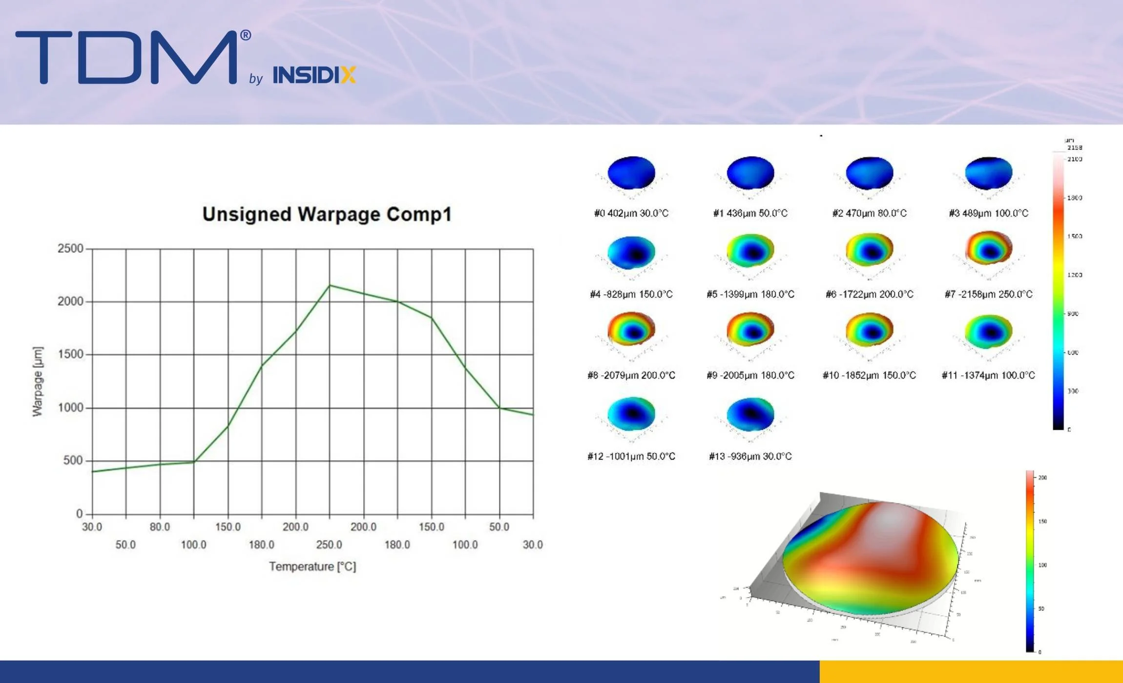
The increasing complexity of modern semiconductor devices necessitates advanced metrology and inspection techniques to monitor and control the planarization process. Optical Coherence Tomography (OCT), a non-destructive imaging technique, has emerged as a powerful tool for this purpose. When integrated into Topography Deformation Measurement (TDM) systems, OCT offers a comprehensive solution for real-time monitoring, defect detection, and process optimization.
Key Benefits of TDM's OCT Module for Planarization and Advanced Packaging
Real-time Monitoring and Process Control:
Surface Topography Tracking: TDM's OCT module provides real-time feedback on surface topography, allowing for immediate adjustments to process parameters to ensure optimal results. Defect Detection: It enables the early detection of critical defects like dishing, erosion, and non-uniformities, preventing potential yield losses.
Precise Thickness and Stress Measurement:
Thin-Film Metrology: The OCT module measures the thickness of thin films and dielectric layers with nanometer-level precision, crucial for advanced packaging technologies.
Stress and Strain Analysis: By analyzing changes insurface topography, it helps identify stress and strain hotspots that could impact device reliability.
Enhanced Process Optimization:
CMP Parameter Optimization: TDM's OCT module enables the optimization of Chemical Mechanical Polishing (CMP) parameters to achieve desired surface finishes.
Reduced Process Variability: By minimizing process variations, it contributes to improved yield and device performance.
Accelerated Time-to-Market:
Rapid Wafer Analysis: The high-speed scanning capabilities of TDM's OCT module accelerate process throughput and reduce time-to-market.
Enhanced Process Efficiency: Optimized process parameters and reduced defects lead to increased manufacturing efficiency.
Lastly, TDM's OCT module has revolutionized planarization and advanced packaging by providing real-time, high-resolution data. This powerful tool empowers semiconductor manufacturers to achieve unprecedented levels of precision, control, and efficiency. As the industry continues to push the boundaries of technology, TDM's OCT module will remain a critical enabler for delivering innovative and reliable semiconductor devices.