
Seeing the Bigger Picture
Seeing the Bigger Picture: Multi-Scale Image + Stitching for Large PCBs
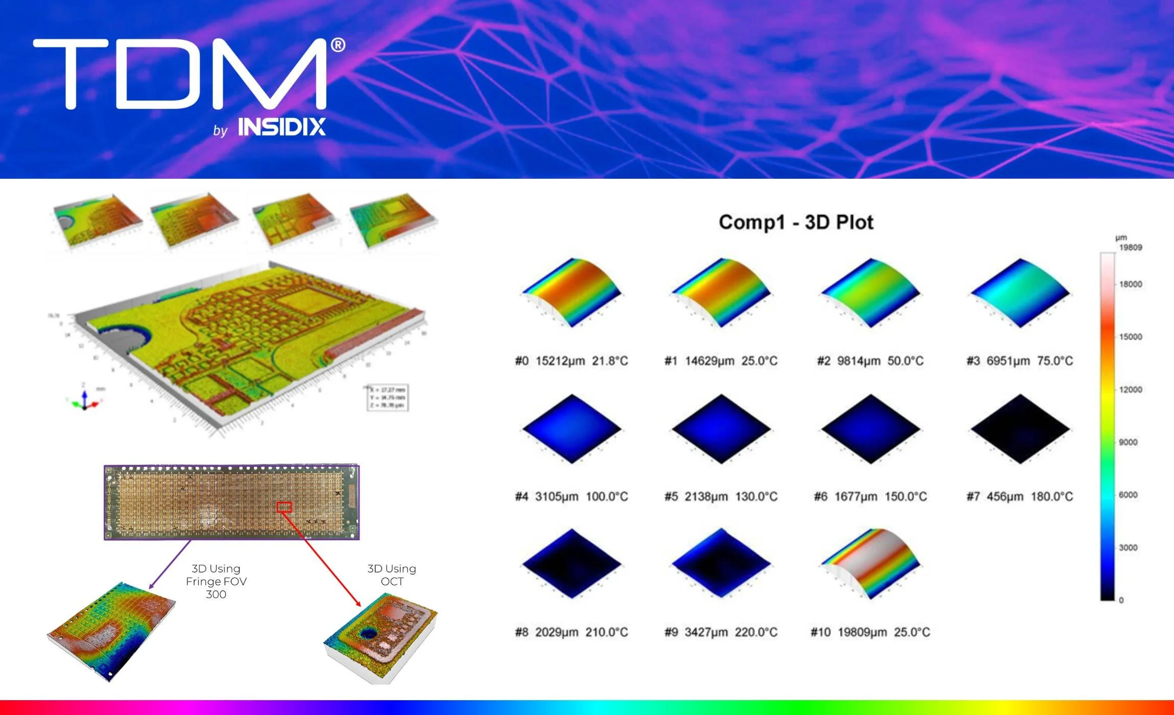
In the ever-evolving landscape of electronics manufacturing, ensuring the quality and reliability of large Printed Circuit Boards (PCBs) is paramount. Traditional inspection methods often struggle to capture the intricate details and overall thermal behavior of these complex devices. However, the advent of advanced imaging techniques, such as multi-scale image stitching, has revolutionized the way we analyze large PCBs.
The Benefits of Multi-Scale Image Stitching
Multi-scale image stitching combines multiple high-resolution images of smaller areas to create a seamless, high-resolution image of a larger field of view. This technique offers several significant advantages:
Enhanced Resolution:By stitching together multiple high-resolution images, the overall resolution of the final image is significantly improved. This allows for detecting fine details, such influenced by hairline cracks, delaminations, and other defects.
Wider Field of View:Multi-scale image stitching enables the capture of large areas, providing a comprehensive overview of the PCB and its components. This is particularly important for identifying potential issues that may affect the overall performance and reliability of the device.
Improved Accuracy:Multi-scale image stitching ensures accurate measurements of critical dimensions and thermal parameters by stitching together images with precise alignment.
Cost-Effective Solution:This technique eliminates the need for expensive, large-format imaging systems, making it a cost-effective solution for analyzing large PCBs.
Flexibility and Adaptability:Multi-scale image stitching can be applied to a wide range of PCB sizes and complexities, providing flexibility in the inspection process.
TDM's Multi-Scale Module: A Game-Changer
TDM's Multi-Scale Module, combined with advanced image stitching techniques, offers a powerful solution for analyzing large PCBs. By capturing high-resolution images of specific areas of interest, the module provides detailed insights into the thermal behavior of the PCB, including temperature distribution, warpage, and stress.
Key Features of TDM's Multi-Scale Module:
High-Resolution Imaging:Captures fine details, such as component placement, solder joint integrity, and thermal hotspots.
Wide Field of View:Enables the analysis of large PCBs, including multi-layer boards and flexible circuits.
Precise Temperature Measurement:Accurately measures temperature distribution across the PCB, identifying potential thermal hotspots.
Automated Image Analysis:Streamlines the inspection process and reduces human error.
By leveraging the power of multi-scale image stitching, TDM's Multi-Scale Module empowers engineers and quality control professionals to ensure the reliability and performance of large PCBs, driving innovation in the electronics industry.